As new RF and microwave systems evolve, we are seeing a greater need for effective thermal management and significantly higher RF performance from Printed Circuit Boards (PCB’s) and subsystems; at the same time these systems are required to decrease in mass and still offer greater functionality than ever before.

Constraints such as these are often most acute in applications where Size, Weight and Power (SWaP) are high priorities, such as military and aerospace, and typically include RF power amplifiers and phased array TxRx modules.
This article reviews the various methods of thermal management and reviews in detail the advantages of “Coin” technology versus traditional thermal via technology.
High density active power devices, such as GaN power transistors, can dissipate significant heat. One of many roles that the PCB has to perform is to channel heat from the underside of the semiconductor device through to the chosen heatsinking scheme as efficiently and effectively as possible.
The design challenge is how best to accomplish this while achieving the other trade- offs required such as RF performance, manufacturability and cost.
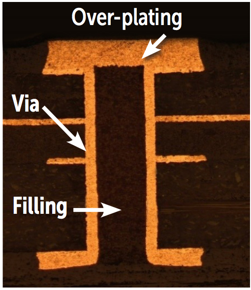
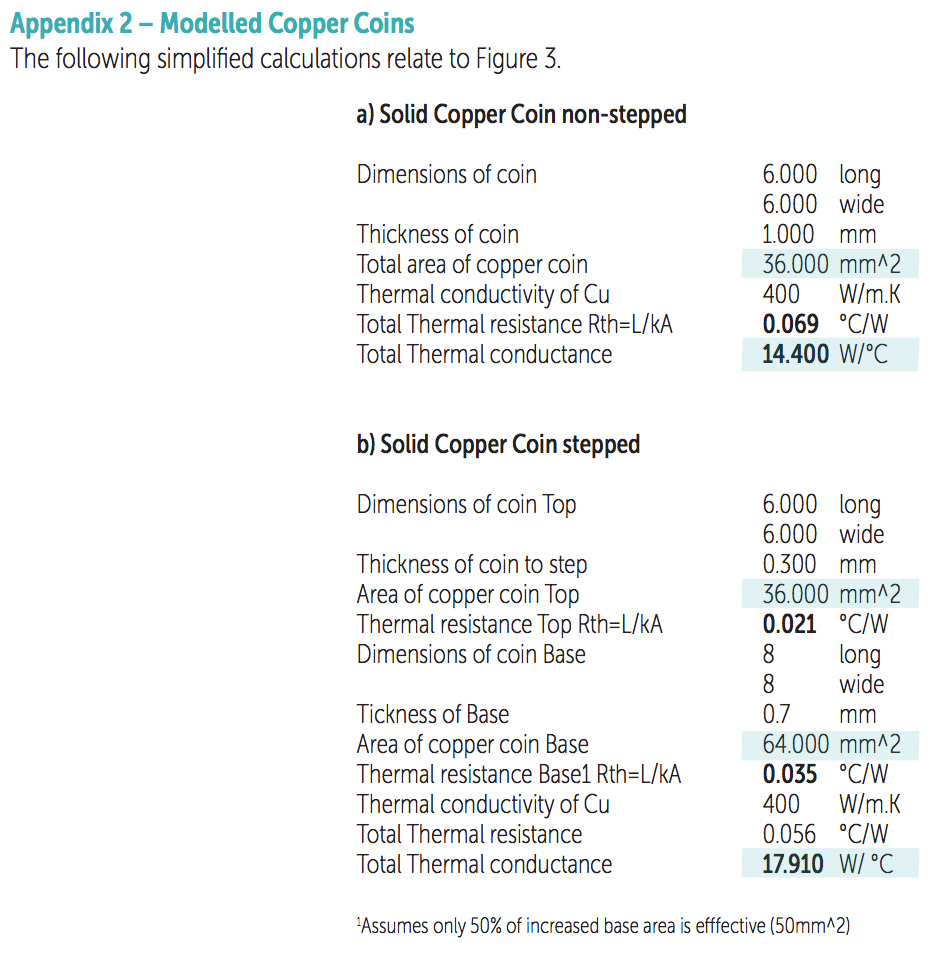
Figure 1a. Cross-section of filled via.
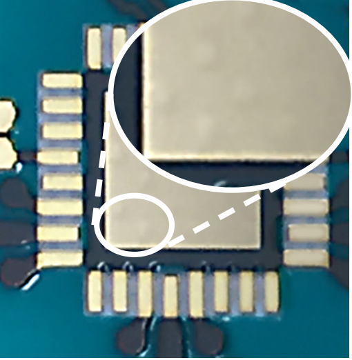
Figure 1b. Photo of typical device ground
pad with overplated vias just visible.
Methods of Thermal Management
Traditionally, designers have simply added plated through holes (PTHs) to thermal/ground pads under components to take heat away through the circuit to a thermal sink such as a cold wall.
Unless the assembly process includes a step to pre-fill these PTHs with solder, there is a high risk that solder will be robbed from under the component into the holes leading to a poor and potentially unreliable connection.
Another solution often used is to have these PTHs under the components filled with a proprietary via plugging paste and plated over the top to give an uninterrupted ground pad.
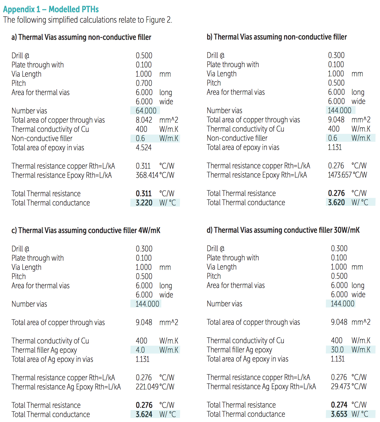
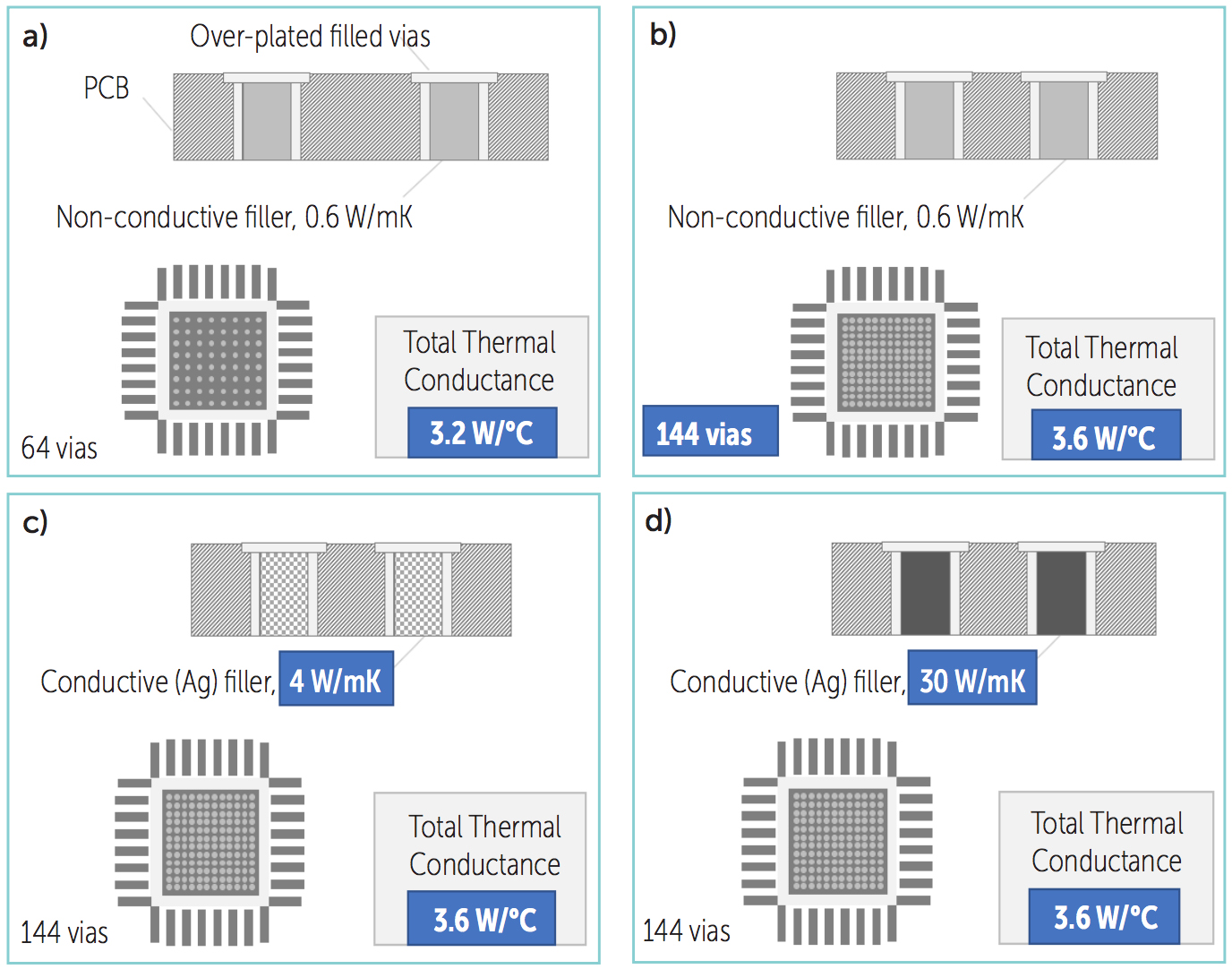 Figure 2: Comparison of total thermal conductance of different filled vias.
The plugging pastes typically used are electrically non-conductive and offer a relatively low thermal conductivity of around 0.6 W/mK compared to a conductivity of copper of 400 W/mK, so do not contribute much to the thermal transfer.
Electrically and thermally conductive paste, for example silver (Ag) loaded epoxy, can be used to fill the thermal PTHs but even with Ag epoxy the thermal conductivity of these pastes is typically in the range of 4 to 30 W/ mK depending upon type — still very low. (See figure 1a) shows an example of a cross section though a filled and over- plated via. (See Figure 1b) shows a typical application with filled thermal vias within the ground pad. Look closely and you will notice subtle outlines of the thermal vias in the central large ground pad.
To improve thermal conductivity, one option is to increase the plated wall thickness of the PTHs from the standard 25um, to 100um, for example. Often a greater number of smaller PTHs within a ground pad can provide a more effective thermal path than fewer larger PTHs.
There are limits to the effectiveness of heat transfer using a traditional ground pad with PTHs.
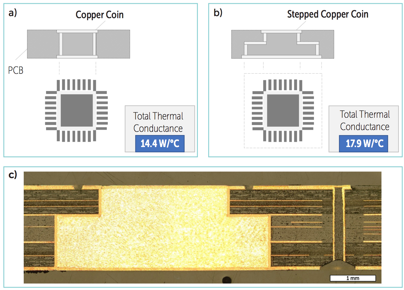 Figure 3: Examples of the use of copper coins.
Figure 2 shows the results of calculations of four different cases, with detailed calculations shown in Appendix 1.
Starting with a typical case of PTHs with 0.1 mm thickness of wall plating1, it examines the overall thermal conductance with vias filled with a non-conductive filler (see Figure 2a).
Using this as the base case, it then examines increasing the number of vias (see Figure 2b), then changes the filling from non- conductive to conductive silver epoxy of two different thermal conductivities (Figure 2c and d).
As can be seen, the benefit of using Ag epoxy instead of standard,
non-conductive plug paste to fill the vias is limited and generally not worth the additional expense.
1While a through-hole wall thickness of 0.025mm is standard in non-thermally challenged applications, we usually recommend 0.1mm where heat transfer is important. Note that if standard 0.025mm plating was used for case 2a, then thermal conductance would only be 0.96 W/°C.
For many leading edge applications the total thermal conductances shown on previous page are not up to the task. A more effective approach is to use copper coins that are integrated into the circuit’s structure.
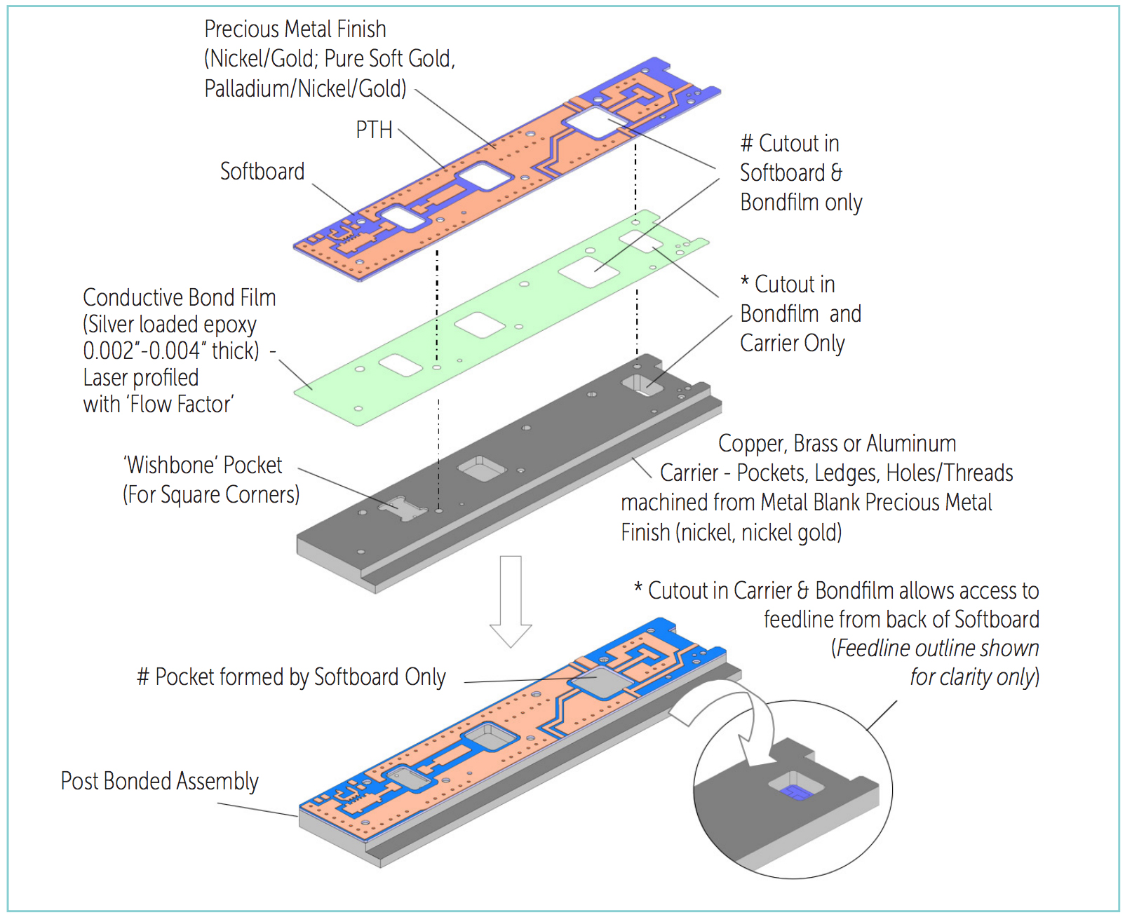 Figure 5: The assembly of post-bonded circuits.
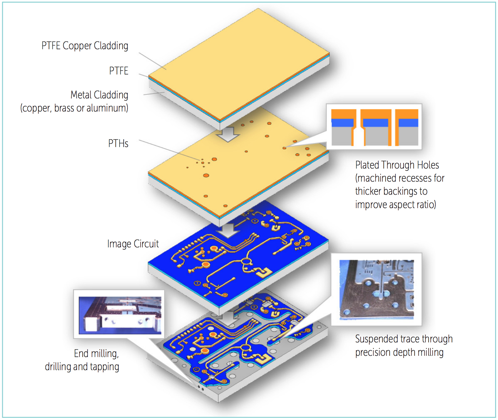 Figure 4: construction of metal-backed circuits.
For ease of comparison, a simple approach is shown in (see Figure 3a), where a 6mm x 6mm square coin is modeled. A more frequently used approach is to have the coin stepped so that heat is not only efficiently conducted away but also spread.
This is modeled in (Figure 3b), and a cross sectional photograph of a real stepped copper coin shown in (Figure 3c). The larger area of copper provides a larger surface area in contact with the cold wall, providing improved thermal transfer. More calculations are given in Appendix 2. Ultimately metal backed circuits offer an ideal solution where large amounts of thermal energy need to be dissipated, as shown in
Figure 4.
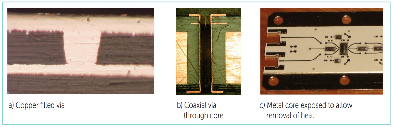 Figure 6: Examples of metal-cored circuits.
The metal backing can be copper, aluminum or brass as this type of circuit is typically used for solid state power amplifiers (SSPA) and can be of either pre-bonded or post bonded structure.
In the case of pre-bonded circuits this is where the substrate is supplied pre-bonded to a thick metal backer. This does limit tracking to a single layer and presents issues during processing as invariably machining operations have to take place after the circuit traces have been formed.
Great care needs to be taken to avoid damaging critical circuit features. The advantage is that this provides an excellent ground plane reference.
The post bonded alternative is easier to manufacture in so much as the circuit is produced and verified before being attached to a pre-machined and plated metal backer as shown in Figure 5.
Post bonded circuits can have more than a single layer of conductors. Generally the circuit is bonded to the metal backer using a conductive adhesive layer.
For both pre- and post-bonded circuits the components that require heat to be transferred away are mounted directly onto the metal backer through openings within the circuit.
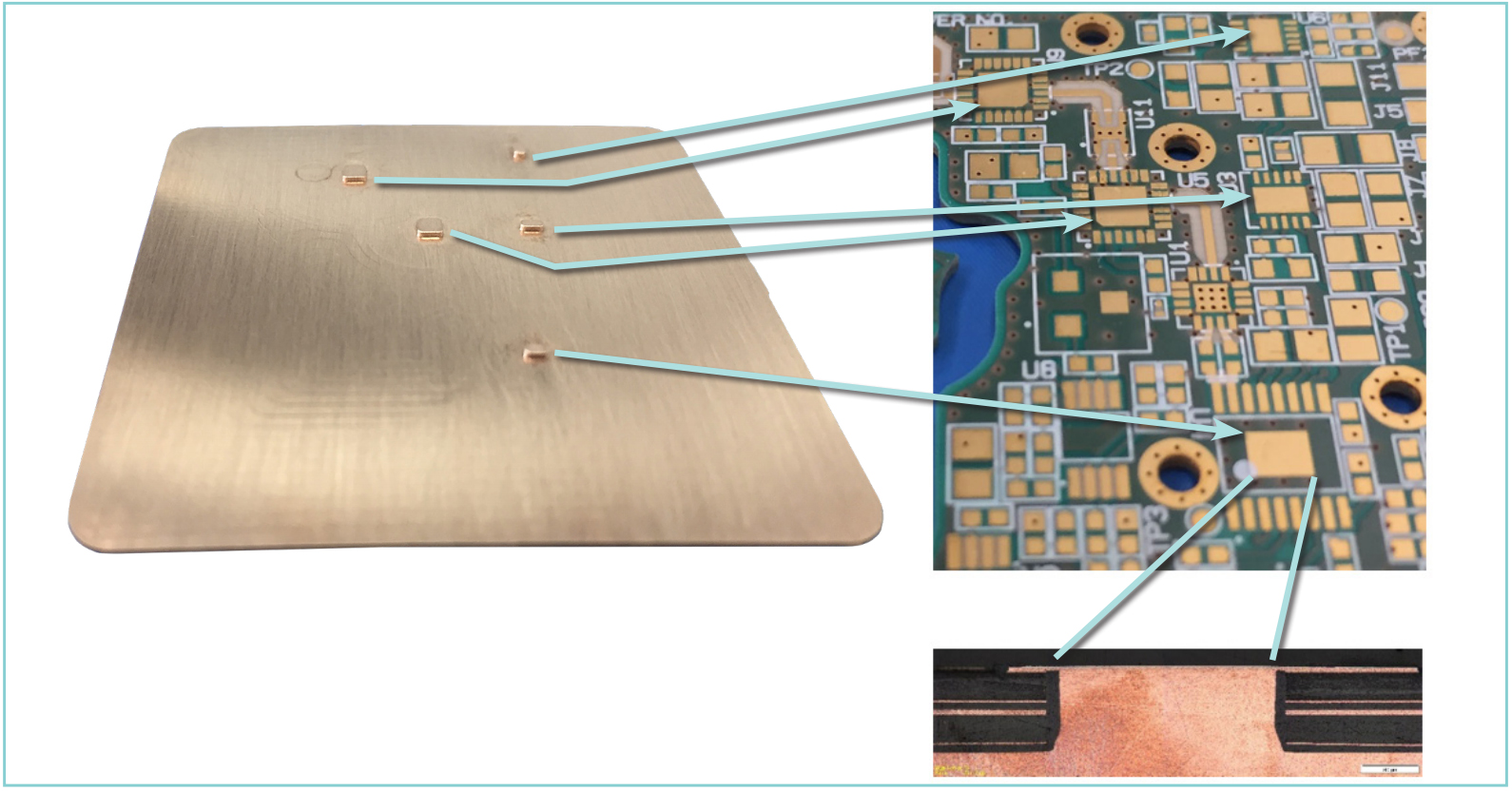 Figure 7: Machined copper plane with up-stands, applicable for small circuits.
A more complex solution is metal-cored circuits. These can be usefully employed where space is limited and high isolation between RF and control is required in addition to thermal management. Heat being transferred from components to the core can either be through thermal vias or by direct contact through cavities within the circuit that the components are mounted on.
Consideration must be given to removing heat from the core. Typically circuit substrate is machined away from two edges to expose the core so it may be clamped within the chassis to transfer heat.
In the case of thermal vias where holes are blind with diameters <0.2mm and depths <0.3mm the holes can be filled with copper using a blind hole plating process. Figure 6 shows examples.
Another technique developed by Teledyne Labtech for thermal management on small circuits (<25cm2) and where the overall thickness is limited, yet several devices require thermal management is to employ a machined copper plane with up-stands (pillars).
This provides an excellent thermal path way and the heat can be distributed efficiently through the thermal plane for transmission to a cold wall. An example is shown in Figure 7.
Summary
For very high power applications, metal backed circuits currently offer the best solution for high power solid state RF devices that are flange mounted; they do not cater well for SMT components requiring thermal management.
Where SMT components with high dissipation requirements are used, coins provide an effective solution for thermal management.
If the required power dissipation is lower, thick walled filled vias offer a lower cost alternative to coins.
Metal core and machined copper planes are generally only employed where space is limited and cost is not the overriding factor. There are thermally conductive substrates available for RF applications but even these generally have rather modest thermal conductivity of typically 1.0 to 1.5 W/mK
For additional information, or for inquiries regarding a specific application, please email ptn_sales@teledyne.com.
www.teledynedefelec.com