The multi-domain battlespace is no longer a future vision. It is a reality now, connecting sensors and shooters through secure and resilient networks. As these systems require increasingly higher levels of reliability, power output and frequency coverage, engineers are turning to high performance materials such as gallium nitride (GaN) to keep up with the evolving requirements.

As a semiconductor material, gallium nitride offers efficiency and high power density, an ideal combination of attributes for radio frequency applications, including radars and electronic warfare systems. Northrop Grumman is using its decades of expertise with GaN and other advanced materials to empower warfighters in their missions.
Advancing the Science of Semiconductors
Fifty years ago, Northrop Grumman opened its Advanced Technology Laboratory (ATL) to create semiconductors for critical military programs. The facility, now a Department of Defense trusted foundry, has delivered more than eight million components that support missions from undersea to outer space and every domain in between. The foundry maintains a wide range of processes in gallium nitride, gallium arsenide, silicon, and silicon carbide in the production of military spec microelectronic chips, some of which are radiation hardened. Nowhere else in the world will you find a single foundry with this broad mix of device fabrication capabilities. A variety of ground-based, aircraft and space systems programs have sourced components from the laboratory.
The ability to move a component through the full design cycle — from mission requirements through to flight test quickly, and all within a two mile radius — makes ATL a unique facility. The lessons learned through that seamless process have transferred to countless Northrop Grumman programs. The company’s experience in developing and integrating GaN into military systems has led to robust capabilities for ground, aircraft and space systems. Northrop Grumman and the government have invested more than $350 million in GaN development.
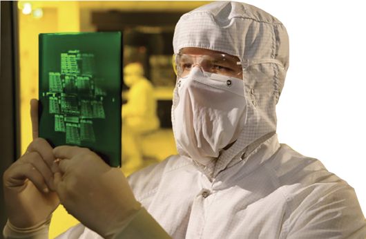
 Inside the Northrop Grumman Advanced Technology Laboratory, which has been in operation for 50 years.
“What we have learned from our work with our cutting-edge Advanced Technology Laboratory is that developing advanced devices is just the beginning,” said Dr. Nicholas Paraskevopoulos, VP, emerging capabilities development, and CTO, Northrop Grumman Mission Systems.
“Ensuring that the device performance will meet or exceed our customer’s expectations once integrated into a complex military system, under challenging real-world conditions, is where our technical team’s expertise makes the difference. This is systems thinking in action.”
One significant example is the Marine Corps AN/TPS-80 program, the first and only multi-mission ground radar in the Department of Defense to use GaN technology. Applied to the AN/TPS-80 radar, GaN enhances system sensitivity and efficiency, increases power density and improves reliability. The system achieved Initial Operational Capability and was fielded last year.
GaN Meets the Law of Large Numbers
Gallium nitride’s ability to provide high power for signal amplification and pulse generation make it a natural fit for many military applications. But defense is not the only field that is taking advantage of the benefits of GaN. The telecommunications industry, currently investing heavily in infrastructure for 5G, is using GaN to power key parts of the network. Those investments are creating positive effects for all users of GaN technology.
The implementation of 5G has created economies of scale for GaN production, driving down prices and increasing the quality and reliability of the components. What was once a specialty item is now approaching commodity status — and that is a good thing, said Rob Howell, a Northrop Grumman fellow and chief technologist.
“Producing GaN components requires hundreds of steps, and ensuring that each one is carried out to specification is critical to the effectiveness of the final product. The investment of commercial industries in GaN has led to a significantly higher process uniformity, from which the military can also benefit,” said Howell.
What’s Next: SLCFET and SiGe
The next generation of microelectronics is taking shape at Northrop Grumman. One technology under development is Super Lattice Castellated Field Effect Transistor (SLCFET), the company’s patented structure that uses GaN to offer even greater levels of performance.

Sensing the Future_3
The SLCFET is a novel device specifically engineered to provide superior ultra-wideband frequency performance for the next generation of military radio frequency (RF) systems.
The device is based on a superlattice of GaN to create parallel, stacked channels of current, which are each controlled by the three dimensional castellated gate, so named due to its resemblance to the top of a castle wall. As RF switch performance is a dominant factor for next generation wideband systems, the SLCFET is a key technology enabler for realizing these future systems.
The company is also a leader in silicon germanium (SiGe) designs, which permit a dramatic reduction in the number of chips required and are ideal for highly integrated RF and mixed signal systems.
With decades of experience in semiconductor design, development and integration, Northrop Grumman provides a range of technologies, including GaN, to power the future of advanced systems in the multi-domain battlespace.
www.northropgrumman.com


